Have you ever wondered how the flow in inkjet printers is controlled, or how car airbags automatically activate during an accident?. All of this and more is done through a very small electromechanical system that can reach few micrometers in size. Besides producing impacts at the macro-level; micro-level sensing, regulating, and reactivating are all possible with this technology, which goes by the name MEMS (micro electromechanical system). The term "transducer" also refers to this system since certain MEMS devices convert a measured mechanical signal into an electrical or optical signal. This mechanism is critical to many fields of technology. It is present in systems for a variety of industries, including communications, electronics, medicine, and military. Auto-adjusting Smartphone screens and HVAC controls are two other instances of MEMS system applications.
There is no doubt that materials science plays a major role in this field, as researchers always seek to search for new materials in the manufacture of sensors in order to obtain greater effectiveness. When selecting materials, considerations include cost, processing simplicity, availability; and, of course, the device's high performance, which means that the material used must have good mechanical and electrical properties.
Materials issues in MEMS:
More and more materials are now accessible for use in micromachining for MEMS devices as a result of research efforts in recent years. However, the quantity of these materials is still restricted because of challenges in the field of micro-fabrication technology. Silicon Si, germanium Ge, gallium Ga and arsenide As are common active substrate materials in MEMS and are all classified as semiconductors. These materials' structure makes them insensitive and stable. Thus, in the realm of sensors, they are indispensable materials.
When silicon is exposed to steam, it easily oxidizes to form a surface layer of silicon dioxide, which is electrically insulating and chemically unaffected. This property sets silicon apart from other active substrate materials. Silicon is well suited for thin-film deposition; it is currently the most commonly used substrate material for MEMS due to its abundance, low cost, and mechanical stability. Additionally, the high Young's modulus of silicon (range from 130 to 188GPa) gives it an excellent elastic property and makes it a resistant material to mechanical stress. Furthermore, before we can examine crystal material properties, we must first establish crystal orientation. A Miller-index is a simple notation used to characterize specific crystallographic planes and directions in a substance. According to Jongpal Kim's and et research, silicon with a Miller-index of (111) is a superior mechanical material for MEMS applications than silicon with an index of (100) or (110); the results of this study indicated that the variation in the bulk shear modulus of the torsion beam for silicon (111) is 4.4 GPa, whereas the values for silicon (100) and (110) are 28.3 and 23.4 GPa, respectively. Silicon (111) has the least variations in bulk shear modulus and is the most resistant to device orientation in terms of crystallographic directions.
Despite all of the benefits discussed, there are some challenges to using silicon in MEMS devices, the most notable of which is the high cost of silicon crystallization. The micro-channels in certain MEMS device applications, like the biomedical industries, have to be longer as the chip size increases. This results in higher chip costs when silicon is used. Silicon is not the best material for bio-sensing, either. In this case, polymers are more biocompatible. In addition, the cost of producing many of the polymers used in this industry is significantly lower than that of crystalline silicon, and some of the polymers can tolerate higher stress levels than silicon.
Another fantastic option for micro electromechanical devices is diamond, which shows exceptional results in terms of stability, chemical inertia, and fatigue resistance. Its large energy gap allows the devices to operate at high temperatures. Diamond possesses exceptional mechanical strength as well; its maximum Young's modulus value is nearly 1,050 GPa, which is significantly greater than that of silicon, which is only 150 GPa. Diamond, on the other hand, has much higher sensitivity due to its extremely high resonance frequencies.
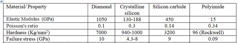
Table.1: Comparison of some mechanical properties of materials used in MEMS ([Made using "MS word"]
.
Two MEMS cantilevers sensors with identical geometry but different materials were created by a team of scientists from CEA, Diamond Sensor Laboratory, ESYCOM, and ISIPCA. Diamond sensors have been found to have higher sensitivity than silicon sensors, based on testing conducted on two different materials: silicon and polycrystalline diamond. The manufactured cantilevers have diamond grains with an average size of 1 μm. Sensor responses were also found to be between 20 kHz and 150 kHz. Furthermore, this study's tests shown that the sensitivity of the sensors increases when polymer layers are utilized to coat microcantilevers.

Figure.1: MEMS microcantilever resonating in an SEM
Diamond provides the best achievements in biological detection due to its carbon-based structure, which allows for the functionalization of particular biological groups.
References:
- Srinivasa Rao Karumuri, K.Girija Sravani, S. Durga SailajaJ.Vijay Sekhar, Y.Srinivas, and Ramendu Bhattacharjee. Micro-Electro-Mechanical-Systems (MEMS) Technology. Archives of Applied Science Research, 2012, 4 (1):307-314. Scholars Research Library. ISSN 0975-508X
- S.M Spearing, Materials issues in microelectromechanical systems (MEMS), Acta Materialia, Volume 48, Issue 1, 2000, Pages 179-196, ISSN 1359-6454
- Singh, Tanvir. (2020). Microelectromechanical System. 10.13140/RG.2.2.27193.60008.
- Jongpal Kim, Dong-il (Dan) Cho, Richard S. Muller. WHY IS (111) SILICON A BETTER MECHANICAL MATERIAL FOR MEMS?. School of Electrical Engineering and Computer Engineering, Seoul National University, San 56-1, Shinlim-dong, Kwanak-gu, Seoul 151-742, Korea, [email protected] - Department of Electrical Engineering and Computer Sciences, University of California at Berkeley, Berkeley, CA 94720-1774, USA
- Matthew A. Hopcroft, Member, IEEE, William D. Nix, and Thomas W. Kenny. What is the Young’s Modulus of Silicon?. JOURNAL OF MICROELECTROMECHANICAL SYSTEMS, VOL. 19, NO. 2, APRIL 2010
- E Kohn, P Gluche, M Adamschik, Diamond MEMS— a new emerging technology, Diamond and Related Materials, Volume 8, Issues 2–5, 1999, Pages 934-940, ISSN 0925-9635
- Rudra Pratap, A Arunkumar. Material selection for MEMS devices- Indian journal of pure and applied physics. Vol. 45, April 2007, pp.358-367
- Possas-Abreu, M.; Ghassemi, F.; Rousseau, L.; Scorsone, E.; Descours, E.; Lissorgues, G. Development of Diamond and Silicon MEMS Sensor Arrays with Integrated Readout for Vapor Detection. Sensors 2017, 17, 1163. https://doi.org/10.3390/s17061163
- Abdellah Massaq, Alexis Rusinek, Maciej Klosak, Slim Bahi, Angel Arias, Strain rate effect on the mechanical behavior of polyamide composites under compression loading, Composite Structures,
Volume 214, 2019, Pages 114-122, ISSN 0263-8223
Thanks for your contribution to the STEMsocial community. Feel free to join us on discord to get to know the rest of us!
Please consider delegating to the @stemsocial account (85% of the curation rewards are returned).
You may also include @stemsocial as a beneficiary of the rewards of this post to get a stronger support.