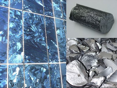
Grey in colour, silicon is a semi-metal that breaks easily. Silica and silicates, which comprise the majority of the Earth's crust after oxygen, are primarily composed of silicon. This component is extremely important in the field of inorganic compounds.
One of the main components of the contemporary electronic revolution is silicon. "Silicon chips" are tiny semi-conductive plates used in the fabrication of electronic circuits. These plates are predominantly made of silicon. Additionally, it has been demonstrated that the photoelectric conversion efficiency of polycrystalline silicon wafers utilised in solar energy applications is very great.
Metal–oxide–silicon transistor:
An abbreviation for a specific type of field-effect transistor (FET) is metal-oxide-semiconductor field-effect transistor (MOSFET). A thin, approximately 0.1 µm-thick silicon oxide (SiO2) insulating layer separates the MOSFET's metal gate from the channel (Figure.3).
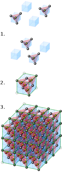
An electrical semiconductor's characteristics are dictated by its atomic configuration. The crystalline structure of silicon matches up to that of diamond, whereby the four atoms at the vertices of a tetrahedral pyramid and each one of the silicon atoms are linked together (Figure.2). Therefore, since there are no free electrons in pure crystalline material, it acts as an insulator at low temperatures.
To induce an excess or deficiency of valence electrons in silicon, dopants such as boron or arsenic are added. Elements such as phosphorus, antimony or arsenic form donor-type impurities, they have five valence electrons, four of which interact with peripheral electrons of silicon atoms, while the fifth remains free to move in the crystal lattice. Therefore, even at low temperatures, there is electrical conduction in silicon crystals that contain impurities.

Figure 3: MOS capacitor on p-type silicon showing inversion and depletion layers
The polarisation of the capacitor created by the gate, channel, and silica layer changes the conductivity of the channel.
Silicon solar cells:
In terms of materials for photovoltaic applications, silicon wafers are still exceptional. Photons can be converted into electronic charges with good efficiency by silicon solar cells, which have demonstrated a strong ability to absorb sunlight.
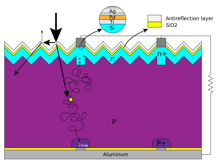
Figure 4: Silicon Solar cell structure and mechanism
Wafers of silicon crystal, measuring 150 microns in thickness, and doped with impurities that have different valence electrons than silicon, are used to make photovoltaic cells. Doping permits the creation of an electric field inside the semiconducting material (p-n junction). A study carried out at CEA revealed that whilst impurities of phosphorus or boron are highly efficient, those of iron and carbon are ineffective and impede the transmission of charges into the two electrodes.
References:
- Metal Oxide Semiconductor (MOS) Transistor Demonstrated". The Silicon Engine. Computer History Museum.
Noor Dzulaikha Daud, Md. Nazibul Hasan, Mohamed Sultan Mohamed Ali, Chapter 9 - Microelectrical discharge machining of silicon wafers, Editor(s): Tanveer Saleh, Mohamed Sultan Mohamed Ali, Kenichi Takahata, In Micro and Nano Technologies, Micro Electro-Fabrication, Elsevier, 2021, Pages 219-244, ISBN 9780128200490 - Les Matériaux au Cœur du Processus d'innovation- Clefs CEA No 59.
- Benyahia Farid, Bruno Bernard- Les Nanosciences et Nanotechnologies. ISBN: 978.9961.0.1663.3
- w. R. Runyan. Silicon Semiconductor Technology. Semiconductor Research and Development Laboratory.
Thanks for your contribution to the STEMsocial community. Feel free to join us on discord to get to know the rest of us!
Please consider delegating to the @stemsocial account (85% of the curation rewards are returned).
You may also include @stemsocial as a beneficiary of the rewards of this post to get a stronger support.
Great article my friend! It reminded me of my basic electronics classes :)
Have a blessed day and Merry Christmas!
Hello , nice to hear that :). And thank you i wish you a Merry Christmas too.