In ancient times, people already knew how to beat the gold into a less than 1 μm thickness with hammers and knew how to use this "gold leaf" for coating all kinds of stuff. And also Nowadays, Many recent discovery and investigated materials which are only available in bulks (Large forms) that believed to be useful in science and technologies are expected to convert to thin forms so that there is reduction of wastage of bulk materials but this thin forms will still retain the same properties and functions of the bulk forms. For example, from the history of first generation of computers, we all know that size of computer is so large that require many hands to move and operate it, but now just imagine how small computer size is and with their great functions and speed. Do you think it’s a magic, CAPITAL NO, All thanks to the part taken by thin film science and technologies. We all need to know basic science of thin film and its applications, so we can realize the beauty of recent thin films science and technologies.
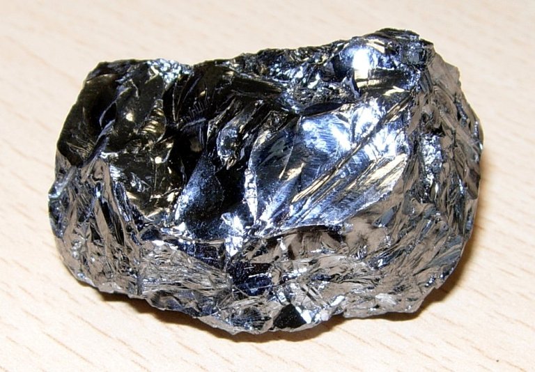
Figure 1: Bulk silicon
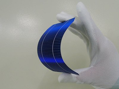
Figure 2: solar cell is a hybrid model that combines a crystalline silicon substrate and an amorphous silicon thin-film
What is thin films?
Thin Film is the layer of material ranging from fractions of a nanometer to several micrometers in thickness. The controlled synthesis of materials as thin films (a process referred to as deposition) is a fundamental step in many applications.
Thin films
What are the purpose of Thin Film development?
- To maintain surface uniformity.
- To reduce the amount (or mass) of light absorbing material.
- Spray Coating Technology for Superior Functional Medical Coatings
- To decrease the weight and bulkiness of the materials
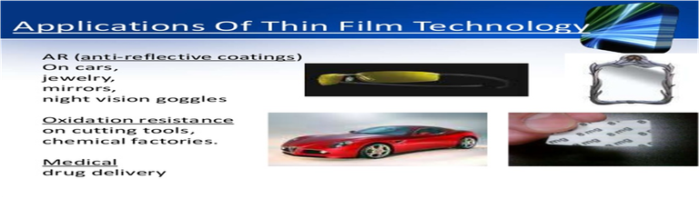
Thin film technology involves deposition of individual molecules or atoms. Advances in thin film deposition techniques during the 20th century have enabled a wide range of technological breakthroughs in areas such as magnetic recording media, electronic semiconductor devices, LEDs, optical coatings (such as antireflective coatings), hard coatings on cutting tools, and for both energy generation (e.g. thin-film solar cells) and storage (thin-film batteries). It is also being applied to pharmaceuticals, via thin-film drug delivery.
Interesting part of thin film is, we can combine two or more materials together on a single thin plate to achieve new and unique properties of materials that believed to be applicable in novel applications such spintronic, magnetic memories, superlattices that allow the study of quantum confinement by creating two-dimensional electron states and so on.
Properties to be considered!
- Proper thickness distribution to meet our specification of materials
- Stability of thin films on substrate
- Proper control of grain size of these thick films
- Controlling the process parameters of deposition.
Deposition: The act of applying a thin film to a substrate (surface) is thin-film deposition – any technique for depositing a thin film of material onto a substrate or onto previously deposited layers.
Types of applying thin film deposition
- PHYSICAL VAPOUR DEPOSITION(PVD): The objective of these deposition processes is to controllably transfer atoms from a source to a substrate where film formation and growth proceed atomistically.
IMPORTANT METHODS :
EVAPORATION SPUTTERING LASER DEPOSITION
LASER (Pulsed Laser Deposition) (Single/Multiphase)
SPUTTERING ( Polycrystalline)
VACUUM DEPOSITION
Chemical vapor deposition (CVD): is the process of chemically reacting a volatile compound of a material to be deposited, with other gases, to produce a nonvolatile solid that deposits atomistically on a suitably placed substrate.
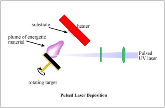
Recently, PLD methods is very common because its less expensive, easy to handle and more accurate compare to others methods.
Pulsed laser deposition (PLD): is a physical vapor deposition technique where a high power pulsed laser beam is focused to strike a target of the desired composition. Material is then vaporized and deposited as a thin film on a substrate facing the target. This process can occur in ultra high vacuum or in the presence of a background gas, such as oxygen when depositing films of oxides.
Reference:
- https://en.wikipedia.org/wiki/Thin_film
- Ingo, G.M.; Guida, G.; Angelini, E.; Di Carlo, G.; Mezzi, A.; Padeletti, G. Ancient Mercury-Based Plating Methods: Combined Use of Surface Analytical Techniques for the Study of Manufacturing Process and Degradation Phenomena. Acc. Chem. Res. 2013, 46, 2365–2375.
- Kuhn, H.; Wilson, B.A. Reflectivity of Thin Silver Films and their Use in Interferometry. Proc. Phys. Soc. Sect. B 1950, 63, doi:10.1088/0370-1301/63/10/302.
- Heavens, O. Optical Properties of Thin solid Films; Dover: New York, NY, USA, 1991.
Congratulations @salawu! You received a personal award!
You can view your badges on your Steem Board and compare to others on the Steem Ranking
Vote for @Steemitboard as a witness to get one more award and increased upvotes!