A light-emitting diode (LED) (pronounced /ˌɛl iː ˈdiː/[1]) is a semiconductor light source. LEDs are used as indicator lamps in many devices, and are increasingly used for lighting. Introduced as a practical electronic component in 1962,[2] early LEDs emitted low-intensity red light, but modern versions are available across the visible, ultraviolet and infrared wavelengths, with very high brightness.
When a light-emitting diode is forward biased (switched on), electrons are able to recombine with holes within the device, releasing energy in the form of photons. This effect is called electroluminescence and the color of the light (corresponding to the energy of the photon) is determined by the energy gap of the semiconductor. An LED is usually small in area (less than 1 mm2), and integrated optical components are used to shape its radiation pattern and assist in reflection.[3] LEDs present many advantages over incandescent light sources including lower energy consumption, longer lifetime, improved robustness,
smaller size, faster switching, and greater durability and reliability. LEDs powerful enough for room lighting are relatively expensive and require more precise current and heat management than compact fluorescent lamp sources of comparable output.
Light-emitting diodes are used in applications as diverse as replacements traffic signals. The compact size of LEDs has allowed new text and video displays and sensors to be developed, while their high switching
rates are useful in advanced communications technology. Infrared LEDs are also used in the remote control units of many commercial products including televisions, DVD players, and other domestic appliances.
HISTORY:-
Discovery and early development:-
Electroluminescence was discovered in 1907 by the British experimenter H. J. Round of Marconi Labs, using a crystal of silicon carbide and a cat's-whisker detector.[4][5] Russian Oleg Vladimirovich Losev independently reported on the creation of an LED in 1927.[6][7]
His research was distributed in Russian, German and British scientific journals, but no practical use was made of the discovery for several decades.[8][9] Rubin Braunstein of the Radio Corporation of America reported on infrared emission from gallium arsenide (GaAs) and other semiconductor alloys in 1955.[10] Braunstein observed infrared emission generated by simple diode structures using gallium antimonide (GaSb), GaAs, indium phosphide (InP), and silicon-germanium (SiGe) alloys at room temperature and at 77 kelvin. In 1961, American experimenters Robert Biard and Gary Pittman working at Texas
Instruments,[11] found that GaAs emitted infrared radiation when electric current was applied and received the patent for the infrared LED.
The first practical visible-spectrum (red) LED was developed in 1962 by Nick Holonyak Jr., while working at General Electric
Company.[2] Holonyak is seen as the "father of the light-emitting diode".[12] M. George Craford,[13] a former graduate student of
Holonyak, invented the first yellow LED and improved the brightness of red and red-orange LEDs by a factor of ten in 1972.[14] In
1976, T.P. Pearsall created the first high-brightness, high efficiency LEDs for optical fiber telecommunications by inventing new
semiconductor materials specifically adapted to optical fiber transmission wavelengths.[15] Up to 1968 visible and infrared LEDs were extremely costly, on the order of US $200 per unit, and so had little practical application.[16] The Monsanto Company was the first organization to mass-produce visible LEDs, using gallium arsenide phosphide in 1968 to produce red LEDs suitable for indicators.[16] Hewlett Packard (HP) introduced LEDs in 1968, initially using GaAsP
supplied by Monsanto. The technology proved to have major applications for alphanumeric displays and was integrated into HP's
early handheld calculators. In the 1970s commercially successful LED devices at under five cents each were produced by Fairchild
Optoelectronics. These devices employed compound semiconductor chips fabricated with the planar process invented by Dr. Jean
Hoerni at Fairchild Semiconductor.[17] The combination of planar processing for chip fabrication and innovative packaging techniques enabled the team at Fairchild led by optoelectronics pioneer Thomas Brandt to achieve the necessary cost reductions.
These techniques continue to be used by LED producers.
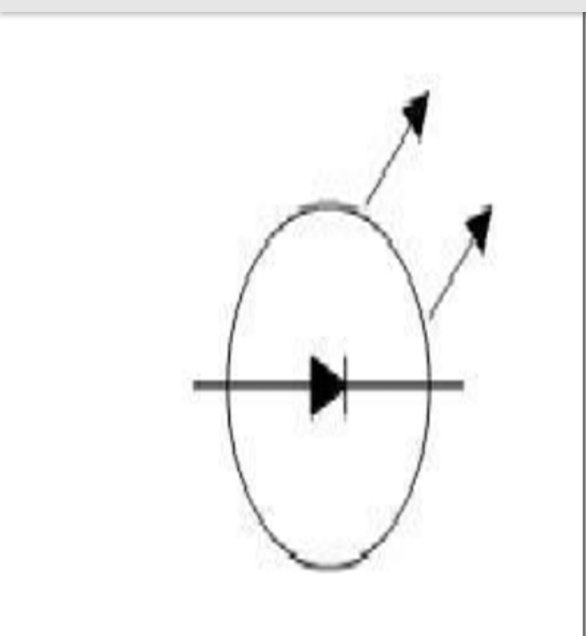
(Schematic diagram of LED)
THEORY:-
A Light emitting diode (LED) is essentially a pn junction diode. When carriers are injected across a forward-biased junction, it emits incoherent light. Most of the commercial LEDs are realized using a highly doped and a p Junction.
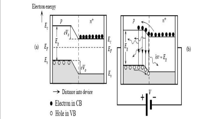
(PN junction diode under biased and unbiased condition)
To understand the principle, let’s consider an unbiased pn+ junction (Figure1 shows the pn+ energy band diagram). The depletion region extends mainly into the p-side. There is a potential barrier from Ec on the n-side to the Ec on the p-side, called the built-in voltage, V0. This potential barrier prevents the excess free electrons on the n+ side from diffusing into the p side. When a Voltage V is applied across the junction, the built-in potential is reduced from V0 to V0 – V. This allows the electrons from the n+ side to get injected into the p-side. Since electrons are the minority carriers in the p-side, this process is called minority carrier injection. But the hole injection from the p side to n+ side is very less and so the current is primarily due to the flow of electrons into the p-side. These electrons injected into the p-side recombine with the holes. This recombination(see Appendix 1) results in spontaneous emission of photons (light). This effect is called injection
electroluminescence. These photons should be allowed to escape from the device without being reabsorbed. The recombination can be classified into the following two kinds:-
• Direct recombination
• Indirect recombination
Direct Recombination:- In direct band gap materials, the minimum energy of the conduction band lies directly above the maximum energy of the valence band in momentum space energy (Figure 2 shows the E-k plot(see Appendix 2) of a direct band gap material). In this material, free electrons at the bottom of the conduction band can recombine directly with free holes at the top of the valence band, as the momentum of the two particles is the same. This transition from conduction band to valence band involves photon emission (takes care of the principle of energy conservation). This is known as direct recombination. Direct recombination occurs spontaneously. GaAs is an example of a direct band-gap material.
(Direct band gap and Direct Recombination)
Indirect Recombination:
In the indirect band gap materials, the minimum energy in the conduction band is shifted by a k-vector relative to the valence band. The k-vector difference represents a difference in momentum. Due to this difference in momentum, the probability of direct electronhole recombination is less. In these materials, additional dopants(impurities) are added which form very shallow donor states. These donor states capture the free electrons locally; provides the necessary momentum shift for recombination. These donor states serve as the recombination centers. This is called Indirect (non-radiative) Recombination. Figure3 shows the E-k plot of an indirect band gap material and an example of how Nitrogen serves as a recombination center in GaAsP. In this case it creates a donor state, when SiC is doped with Al, it recombination takes place through an acceptor level.
The indirect recombination should satisfy both conservation energy, and momentum. Thus besides a photon emission, phonon(See Appendix 3) emission or absorption has to take place. GaP is an example of an indirect band-gap material