For simplicity, we can divide engineering materials into three main categories: metallic materials, polymeric materials, and ceramic materials. But this work will focus on the effect of temperature on the conductivity of the metallic material (conductors) and semiconductors.
It is a known fact that conductors allow free flow of electrons with very little application of pressure such as from a voltage source. Some of the examples of conductor include silver, copper, aluminium etc. Insulators on the other inherently have few electrons, high stability and density coupled with low mobility and as such a massive potential difference is needed to produce any sizable current.
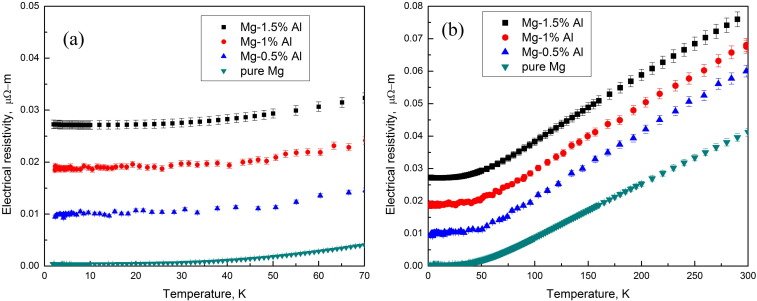
Source: Effect of temperature on the electrical resistivity of magnesium
It is worthy to have it in mind that even the best of insulators will break down (permit charge to flow around and through it) if we apply sufficiently large potential to it. Example of such material include polyethylene, polystyrene. Plastic, paper, mica etc.
We must remember that material usage and engineering designs are continuously evolving. This change continues to speed up. It is difficult to predict to certainty the long-term future advances in material design and usage. In 1943, the prediction was that successful majority of people in the United States would own their auto-aeroplanes which turned out to be a wrong prediction when you look at the fact that the transistor, the integrated circuit were all neglected.
Thirty years ago, it would have been hard to believe that someday computers would become a common household item similar to a telephone or a washing machine.
Semiconductors are elements having a conductivity that lies in-between that of a good conductor and that of an insulator.
In general, semiconductor materials fall into one of the two classes; single-crystal and compound,(consisting of two elements).
Single-crystal semiconductors such as Germanium (Ge) and Silicon (Si) have a recurring crystal structure, whereas compound semiconductors such as Gallium Arsenide (GaAs), Cadmium Sulfide (CdS) Gallium Nitride (GaN) and Gallium Arsenide Phosphide (GaAsP) constitutes two or more semiconductor materials of different atomic structures.
The three semiconductors that are widely used for the construction of electronic devices are Ge, Si, and GaAs.
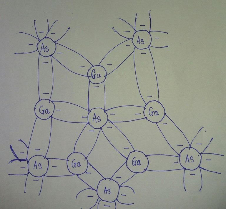
Fig: Covalent bonding of the GaAs crystal
To fully appreciate why Si Ge and GaAs are the semiconductors of choice for the electronics industry, it requires some understanding of the atomic structure of each and how atom are bound together to form a crystalline structure. Every atom is composed of three basic principles: electron, the proton and the neutron. In lattice structure, neutrons and protons form the nucleus and electrons appear in fixed orbits around the nucleus.
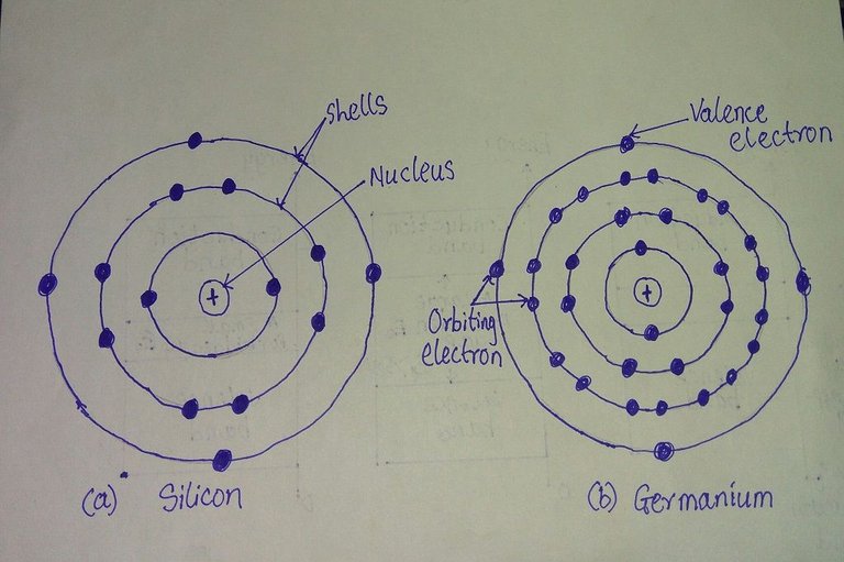
Fig:Atomic structures of (a) Silicon and (b) Germanium
As shown here, silicon has 14 orbiting electrons, germanium has 32 electrons, gallium has 31 electrons, and arsenic has 33 orbiting electrons.
For germanium and silicon, we refer to the four electrons in the outermost shell, as valence electrons. Germanium has three valence electrons, and Arsenic has five valence electrons. Atoms that have four valence electrons are called tetravalent, those with three are called trivalent, and those with five are called pentavalent. The term valence is used to indicate that the potential (ionisation potential) required to remove any one of these electrons from the atomic structure is considerably lower than that required for any other electron in the structure.
Covalent bonding is the primary atomic bonding. Whereas ionic bonding involves highly electropositive and electronegative atoms, covalent bonding takes place between atoms with a small difference in electronegativity and which are close to each other in the periodic table. In covalent bonding, the atoms most commonly share their outer ‘’s’’ and ‘’p’’ electron with other atoms so that each atom attains the noble-gas electron configuration. In a single covalent bond, each of the two atoms contributes one electron to form an electron-pair bond, and the energies of the two atoms associated with the covalent bond are lowered because of the electron interaction.
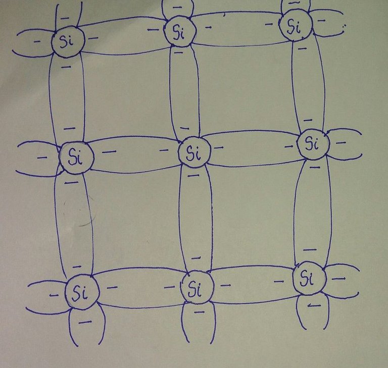
Fig: covalent bonding of the silicon atom
In a pure silicon or germanium crystal, the four valence electrons of one atom form a bonding arrangement with four adjacent atoms.
Although the covalent bond will result in a stronger bond between the valence electrons and their parent atom, it is still possible for the valence electrons to absorb sufficient kinetic energy from natural causes to break the covalent bond and assume “free” state.
The term free is applied to any electron that has separated from the fixed lattice structure and is very sensitive to any applied electronic fields such as established by voltage sources or any difference in potential.
The intrinsic semiconductor material is semiconductor material that was produced and refined to have a minimal level of impurities with purity level that can be harnessed from the available technology.
The electrons in a material due to only external causes are referred to as intrinsic carriers. The number of carriers in the intrinsic material such as relative mobility of the free carriers in the material dictates the ability of the free electrons to move throughout the material.
It is proven that GaAs has the greatest mobility, as compared to Si and Ge, a factor which endears it to such application requiring fast response times. Si has the least mobility whose mobility is almost half of what is obtainable with Germanium (Ge).
One of the most important technological advances of recent decades has been the ability to produce semiconductor materials of high purity which was the factor the use of Si at the onset. It was easier to create germanium of the required impurity level. Impurity level of 1 part in 10 billion is obtainable today.
One might wonder the need to produce the semiconductor at the highest level of purity. It is certainly important when you put into consideration that the addition of one part of impurity (of the right type) per million in a wafer of silicon material can change it from a relatively poor conductor to a good conductor of electricity.
The ability to change the characteristics of material through the introduction of impurity to an intrinsic carrier is called doping, which can readily be applied to GaAs, Ge, Si to improve their conductivity.
One important and interesting difference between semiconductors and conductors is their response to the application of heat. For conductors, the resistance increases with an increase in heat. The number of carriers in a conductor does not increase considerably with temperature, but the positive-ion core vibrates about a relatively fixed location makes it increasingly difficult for a sustained flow of carriers through the material. Materials that react in this way are said to have a positive temperature coefficient.
Semiconductor material, however, exhibit an increased level of conductivity with the application of heat. As temperature rises, an increasing number of valence electrons absorb sufficient thermal energy to break the covalent bond and to contribute the number of free carriers necessary to facilitate conduction. Therefore semiconductor material has negative temperature coefficient
In metallic solids, the atoms are arranged in a crystal structure and are bound together by their outer valence electrons by metallic bonding. The metallic bond in solid metals makes the free movement of the valence electrons possible since they are shared by many atoms and are not bound to any particular atom. Sometimes the valence electron is visualised as forming an electron charge cloud.
At room temperature, the positive-ion cores have kinetic energy and vibrate about their lattice positions. With increasing temperature, these ions vibrate with growing amplitudes, and there is a continuous interchange of energy between the ion cores and their valence electrons.
This vibration could be visualised thus: let us assume that the electron is a car moving in one direction while the ion cores are stationary cars packed on the road. The moving car (electron) will find it easy to manoeuvre through the stationary cars and progress.
Now with increase in temperature, the original stationary cars (positive-ion cores) would now be energized and tends to move slowing opposite the oncoming car and as such impeding the movement of the oncoming vehicle. This disturbance is precisely what happens to the electron and, once the electron movement is slowed, conductivity reduces and gives rise to increase in resistivity.
In the absence of an electric potential, the motion of the valence electrons is random and restricted, so there is no net electron flow in any direction and thus no current low. In the presence of an applied electric potential, the electrons attain a directed drift velocity that is proportional to the field.
Energy-Band Model For Insulators
In insulators, electrons are tightly bound to their bonding atoms by ionic or covalent bonding and are not free to conduct electricity unless highly energized. The energy band model for insulators consists of a lower filled valence band and an upper empty conduction band. These bands are separated by a relatively large energy gap E. To free an electron for conduction, the electron must be energised to jump the gap which may be as much as 6 to 7 eV as, for example, in pure diamond. In diamond, the electrons are tightly held by sp3 tetrahedral covalent bonding.
Intrinsic semiconductors
The mechanism of electrical conduction in intrinsic semiconductors
Semiconductors are materials whose electrical conductivities are those of highly conducting metals and poorly conducting insulators. Intrinsic semiconductors are pure semiconductors whose electrical conductivity is determined by their inherent conductive properties. Pure elemental silicon and germanium are intrinsic semiconducting material.
Electrical charge transport in crystal lattice of pure silicon
In the electrical conduction process in a semiconductor such as pure silicon or germanium, both electrons and holes are charge carriers and move in an applied electric field. Conduction electrons have a negative charge and are attracted to the positive terminal of an electrical circuit. Holes, on the other hand, behaves like positive charges and are attracted to the negative terminal of an electrical circuit. A hole has a positive charge equal in magnitude to the electron charge.
The motion of hole can be visualised by referring to the figure below. Let a hole exist at atom A where a valence electron is missing, as shown in the diagram below. When an electric field is applied in the direction shown in fig below, a force is exerted on the valence electrons of atom B, and one of the electrons associated with atom B will break loose from its bonding orbital and move to the vacancy in the bonding orbital of atom A, the hole will now appear at atom B and in effect will have moved from A to B in the direction opposite to the applied field.
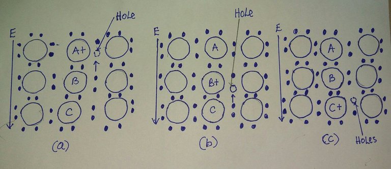
Fig: Schematic illustration of the movement of holes and electrons in a pure silicon semiconductor during an electrical conduction caused by the action of an applied electric field
By a similar mechanism the hole is transported from atom B to C by an electron moving from C to A, which is in the direction of the applied field, and a hole is transported from A to C, which is in the direction of the applied field.
Thus, during electrical conduction in a pure semiconductor such as silicon, negatively charged electrons move in the direction opposite to the applied field (conventional current flow) and toward the positive terminal and positively charged holes move in the direction of the applied field toward the negative terminal.
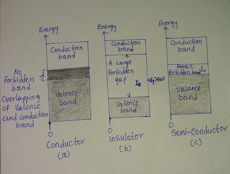
Energy-band diagram for conductor, insulator, and semiconductor
Energy-Band Diagram For Intrinsic Elemental Semiconductors
Energy band diagram is another method of describing the excitation of valence electrons to become conduction electrons in semiconductors. For this representation, only the energy required for the process is involved, and no physical picture of the electrons moving in the crystal lattice is given.
In the energy band diagram for intrinsic elemental semiconductors (for example, Si or Ge), the bound valence electrons of the covalently bonded crystal occupy the energy levels in the lower valence band.When the electrons gain energy from the surrounding environment, the electrons can be lifted from the valence band to the conduction band. The forbidden energy gap is so narrow that the energy needed to achieve movement is 1 eV. The energy needed for an electron to escape the valence band to the conduction band is around 1.1 eV (Si) for silicon, 0.67 eV (Ge) for germanium, 1.41 eV (GaAs) for Gallium arsenide.
REFERENCES
Thanks for sharing. You seem dedicated to educating folks on electricity and electronics. Really commendable work and very clear explanation as always. I particularly like how you explained why semiconductors exhibit decrease in resistance with increase in temperature as compared to conductors whose resistance increase with increase in temperature.
Well done!
I can't thank you enough for finding time to go through the post. Semiconductors are the backbone of modern electronics. The development of high speed computers is the product of evolution of semiconductor.Also the high performance of communication system was hinged on improvement in semiconductor electronics.