

Hello steemians! Feel relaxed as I discuss the remaining sections in building an android phone controlled moving LED display. Did you miss the section earlier discussed? Relax your nerves! Check it out here: .
The system design if of five stages. One of the stages (LEDs array stage) has been discussed extensively in my previous article. The other four stages are Shift Register, Bluetooth, Power/Drivers and Micro-controller stages.
STAGE 2: SHIFT REGISTERS STAGE

Components needed
- 8 pieces of Shift register Integrated circuit (SN74HC595).
- 16-pin integrated circuit socket to house the eight shift registers.
- jumper wires.
For 64x7 LEDs arrangement which this design is all about, 8 shift registers, specifically the SN74HC595 will be used (since 8 columns-7 rows can only use one shift register). The shift register has 16 pins. This type of shift register is an 8-bit serial-in, serial or parallel-out shift register with output latches. This means that you can send data in to the shift register in series and send it out in parallel. In series means 1 bit at a time. Parallel means lots of bits (in this case 8) at a time. Data is entered when the LATCH is set to LOW (this allows data to be sent to the chip) and sent out when the LATCH is set to HIGH. So you give the shift register data (in the form of 1’s and 0’s) one bit at a time, then send out 8 bits all at the exact same time.
Each bit is shunted along as the next bit is entered. If a 9th bit is entered before the Latch is set to HIGH, then the first bit entered will be shunted off the end of the row and be lost forever. Shift registers are usually used for serial-to-parallel data conversion. In this case, the data that is output is 1’s and 0’s (or 0V and 3.3V), so you can use it to turn on and off a bank of eight LEDs.
All the 64 columns from the LEDs array are then connected to the predefined pins (15,1,2,3,4,5,6,7) in each of the 8 shift registers, as discussed in LEDs array stage in PART 1 of this article. All the pin 8s and 13s of the 8-shift registers are connected together to ground (negative power supply). Pin 16s and 10s are joined together for all the shift register and are given a 3V. Pin 9s and 14s are joined together and are connected to digital pin 11 of the micro-controller. Pin 12s are all joined to pin 8 of the controller. Pin 11s of the shift registers are all joined to pin 12 of the micro-controller.
Imagine the Latch as a gate that will allow data to escape from the SN74HC595. When the gate is lowered (LOW), the data in the SN74HC595 cannot get out, but data can be entered. When the gate is raised (HIGH), data can no longer be entered, but the data in the Shift register is released to the eight pins. The Clock is simply a pulse of 0’s and 1’s, and the Data Pin is where you send data from the Arduino to the SN74HC595.
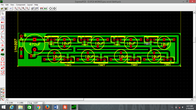
shift registers arrangement on a printed circuit board
.png)
Source: drew by me (@thestronics) with ExpressPCB software
STAGE 3 : POWER SUPPLY AND DRIVERS STAGE
- POWER SUPPLY UNIT:
.png)
Source: drew by me (@thestronics) with proteus software
As the name implies, this is the unit from which the maximum of 5V dc voltage ever needed in the circuit is being supplied. This design employs an uninterrupted power supply (UPS) design which ensures that the scrolling display is always powered. The UPS design employed ensures that required 5V is always available; generated from the rechargeable battery embedded in the scrolling display. Power consumed (estimated) by other associated circuitry is calculated thus:
The micro-controller sources current to drive outputs from 7 pins of its input and output pins with each pin outputting maximum of 50mA.
Eight (8) shift registers would be used in this design with each consuming an estimated current of 50mA at 5V. Hence, maximum total power consumed by the scrolling display unit would be a total of the power consumed by the LED array and the associated circuitry.
As shown above , the mains supply source which is used to charge the battery comprises the following components.
A transformer which steps down the a.c supply voltage to suit the requirement of the solid-state electronic devices and also provides isolation from the supply line.
A full wave bridge rectifier which performs the transformation of the a.c. voltage into a pulsating d.c. voltage in a process known as rectification.
Capacitors which filter out (remove) fluctuations or pulsations (called ripples) present in the rectifier output voltage.
A fixed 1C voltage regulator (7805) mounted on the internal circuit board to provide a stable + 5V d.c. output from the unregulated 12V d.c. fed into its input from the a.c/d.c. adapter. The filtering capacitor should not discharge down to any value below 7v in accordance with the specifications of the input voltage to 7805 voltage regulator. A capacitor of value twice the one calculated(1027uF) is used for filtering. This ensures the safe state of the circuitry. The nearest available capacitor value of 2,200µF (electrolytic) is used as the filter capacitor. The output from the electrolytic capacitor is fed to the input of the 7805 which outputs 5V needed to power the micro-controller circuitry.

An electrolytic capacitor is one of the types of capacitors that makes use of an ionic conducting liquid as one of its parallel plates. The capacitor has a very high value of capacitance per unit volume than any varieties of capacitors. That's why they are made used of in low-frequency and high current electric circuits. They are also widely used as coupling capacitors in circuits where AC but not DC should be conducted. Electrolytic capacitors have a very high capacitance, allowing filters made with men to have very low corner frequencies.
DRIVERS UNIT
This unit is made up of 10uF capacitors and 7805 voltage regulator which drive column of the particular LED(s) to be turned on through the supply of an active low at the cathode of the LED concerned. Total current consumption per column is given by current consumption per LED x total number of LEDs on a column. The display unit is designed to consist of four display modules each consisting of 7x16 LED matrix, thus giving an array of 7 x 64 LED matrix at large, that is 448 LEDs altogether. It must be stated here that 7 rows have been used because it is easier to keep the number of rows equal to the height of the ASCII character (7) thus reducing the firm ware complexity considerably.
The anodes of all LEDs in the same row for each board are connected together while the cathodes of all LEDs in the same column are likewise connected together. The lines connecting the anodes on each of the 7 rows constitute the date lines while the lines connecting the cathodes of the LEDs on each of the 16 columns are the address lines.
This arrangement leads to having seven data lines per module, giving 28 data lines in all while there are 16 address lines of each board are connected together. The 150 0hm resistors are serving as current-limiting devices to prevent the connected LEDs from drawing excessive current and getting destroyed. The 150 value used is justified thus; since the maximum current to power an LED is 30mA and the needed voltage being between 1.5 to 3.3V, then using safe values of 20mA and 3V. The 3V output from each 150 ohm resistor is connected to power pin 10s and 16s of each shift registers.
drivers unit pcb
.png)
source : drew by me (@thestronics) with ExpressPCB software.
STAGE 4: BLUETOOTH STAGE.

A Bluetooth is a wireless device that uses short-wavelength Ultrasonic High Frequency (UHF) radio waves, majorly 2.4 - 2.485GHz for data exchange within short distance range (100 meters).In this project, I'm making use of the HC-05 type of Bluetooth technology. The device has six terminals, four of which will be interfaced with the microcontroller pins. These four terminals are GND, VDD, TX and RX. GND terminal is given 0V, VDD is given 5V. RX is interfaced with TX (pin3) of the controller while TX terminal of the Bluetooth is intefaced with the RX(pin2) of the controller. This arrangement is what is known as Serial communication between the Bluetooth device and the microcontroller and is as shown below:

source : @thestronics
SPP Pro Bluetooth Application is connected with the design and the desired characters to be displayed on the LEDs are typed on the Application interface.
STAGE 5: MICRO-CONTROLLER STAGE.
.png)
source : drew by me (@thestronics) using ExpressPCB software
This stage is made up of the ATMEG-328, which controls the activities of all other circuitry. The micro-controller's board has beside it a master shift register IC (SN74HC595) which controls all other shift registers earlier mentioned in stage 2. The board also comprises ULN2003 IC that takes in all inputs of the 7 rows from the LEDs array.
ULN2003 is simply a monolithic high current and high voltage Darlington array of seven NPN Darlington pairs with a very high-voltage outputs. . In this case, it's used as a driver (to drive the cathodes of the LEDs array). It operates on 5V CMOS devices. Row 1 of the LEDs array is connected to pin 16 of the ULN2003, row 2 to pin 15, up to row 7 to pin 10. The collector-current rating of one Darlington pair is about 500MA
REFERENCES
THANKS FOR READING!!!
