
The most important applications of semiconductors in electronics are based on properties of junctions of semiconductors with different types of conductibility, and junctions of semiconductors with other materials.
A junction ofp-type and n-type semiconductor is called a pn-junction and represents simple semiconductor element - semiconductor pn-diode. Except pn-diode, pn-junction is basis for more complicated semiconductor elements like bipolar transistor and unijunction transistor. Therefore understanding physical effects of pn-junction is necessary for understanding the work of those elements.
Structure of pn-diode
In the base of p-type semiconductor there is technologically formed layer of n-type semiconductor. Diode can also be realized with forming a layer of p-type semiconductor in a n-type base. The boundary between the p and n type semiconductor is representing pn-conjuction.
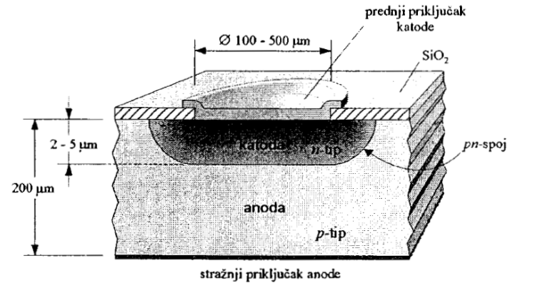
P type base represents anode and n type area represents cathode. The cathode is covered in metal whereas a connector is formed. The rest of the surface is covered in layer of silicon dioxide (SiO2) which is an insulator.

Pn-junction equilibrium and depletion layer
With the junction of p and n type semiconductors a new structure is created. On one side there is a large number of holes and only a few electrons, while on the other side the situation is opposite.
Because of the big difference in concentrations of carriers of the same type on both sides of the junction, diffusion of carriers occurs in the moment of contact. Holes travel from p to the n side, while the electrons travel from n to p side. That is why diffusion currents Idp and Idn start to exist.
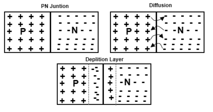
Holes recombine with the electrons, and electrons recombine with the holes. Therefore, in the environment of the pn-junction, a narrow area without movable charge carriers is created, a depletion layer.
Depletion layer is also an area with spatial charge. Electrons from the n side of depletion layer have recombined with the holes and the leftover are positively ionized donor impurities. In the same manner, the p side of the layer creates negative spatial charge. Consequently a difference in potential of two sides of depletion layer is created and that is why an electrical field F whose direction is from the n to the p side starts to exist.
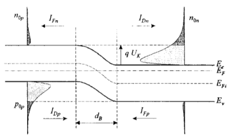
Because a connection between energy E and potential ψ exists, the difference in the potential inside the depletion layer implies that an energy difference between p and n sides also exist. As the p side is more negative, energies of the p side are higher than the ones of the n side. In quasi-neutral regions outside of the depletion layer energies are constant.

The difference between the energy levels is qUk where Uk is contact potential and q is carrier charge. The shift in energies causes an energetic barrier appear which resists the mainstream flow of the majority carriers to the other side. Only a small insignificant number of carriers, with the energy greater than qUk, manages to overcome the barrier and diffuse to the other side in the state of balance.
Pn-junction polarization
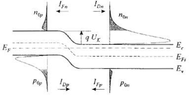
In the state of balance, a current is not flowing through the pn-junction because of the energy barrier (qUk).
Foward bias
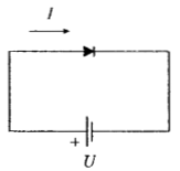
If there is a positive charge U between cathode and anode it will reduce the difference in the depletion layer. Lowered difference results in lowered energy barrier. Number of majority carriers that can cross from one side to the other is greater. Diffuse currents of majority carriers are greater than drift currents of minority carriers and there is a current flow through the pn-junction.
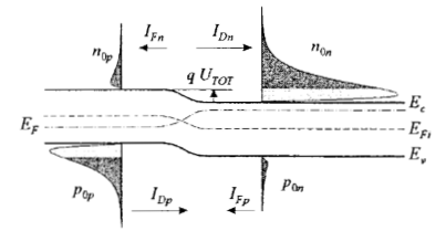
Further increase of the positive U charge results in lower energy barrier and increased current. That ensures good conductibility of the pn-junction and that polarization is called forward bias.
Reverse bias
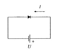
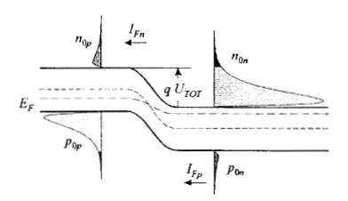
If there is a negative charge U between cathode and anode it will enlarge the difference in the depletion layer. Greater difference results in higher energy barrier. Number of majority carriers that can cross from one side to the other is lowered. Diffuse currents of majority carriers are lower than drift currents of minority carriers and there is no current flow through the pn-junction (except for the drift currents which are insignificant and constant regardless of the bias).
Summary
A p–n junction diode allows electric charges to flow in one direction.
When the pn–junction is forward-biased, electric charge flows freely due to reduced resistance of the pn–junction. When the pn–junction is reverse-biased, the junction barrier becomes greater and charge flow is minimal.
Pn-junctions are elementary "building blocks" of most semiconductor electronic devices such as diodes, transistors, solar cells, LEDs, and integrated circuits. Therefore understanding physical effects of pn-junction is necessary for understanding the work of modern semiconductor electronic elements.
In the next post I will talk about few pn-junction applications like a common type of transistor, the bipolar junction transistor, which consists of two p–n junctions in series, in the form n–p–n or p–n–p.
Thank you for reading.
Unless you made your images you really need to include references! Thanks!
Also gramatically your title would read better as "What are transistors made of"
Thank you for the feedback.
I changed the title and will reference images in the future.
I do not understand everything, but I think you did a good post. However, there is no reference about images
Not citing the source of photos(images) is plagiarism. Here is a post on why this is bad, and here is how easy it is to find allowed photos.
Creative Commons: If you are posting content under a Creative Commons license, please attribute and link according to the specific license. If you are posting content under CC0 or Public Domain please consider noting that at the end of your post.
If you are actually the original author, please do reply to let us know!
I am not the author of the pictures.
I apologize for the inconvenience that I've caused.
Further image usage will contain a proper reference.
Thank you for your feedback.
I have recently read that scientists are chemically growing transistors. Our future in electronic technology is about to dynamically change. http://newscenter.lbl.gov/2016/07/11/atomically-thin-transistors/
excellent, I always liked electronics, congratulations
❤ ✔